博文

目前显示的是 六月, 2021的博文

Where Can Flexible PCB be Used in Medical Devices?

图片
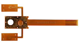
      Flexible PCB   has the advantages of space saving design, light weight and cost saving. Moreover, it can reduce the usage amount of routing by 75% and the cost of electrical interconnection by 70%. These advantages make them suitable for high-precision medical device. So where can flexible PCB be used in medical device? Medical device screens: The transfer cables on the medical equipment screens are all flexible PCBs, which are not only used for medical treatment, but also flexible PCBs are used for transfer cables on the screen displays of almost all equipment, , which is an affirmation of flexible PCBs.     Medical device buttons: Flexible PCBs are widely used in buttons, because flexible PCBs have good flexibility.     B-scan ultrasonography: B-ultrasound is a super strong signal flow penetrating the human body to perform a perspective of the inside of the human body. The flexible PCB with electronic components can accurately transmit the signal, and the signal screen frequenc

What Should We Pay Attention to When Using Ceramic PCB?

图片
  Nowadays, with its own advantages,  ceramic PCB  has been widely used in high-power power electronic modules, solar panel components, high-frequency switching power supplies, automotive electronics, aerospace, high-power LED lighting products, automotive sensors and other fields. Not only that, it also plays a vital role in home life.   In addition, if we want to make the use of ceramic PCB better, we need to pay attention to the following points.   1.  Heat ing  pretreatment before wire bonding Since the ceramic PCB has been processed by laser, only through reasonable heating pretreatment can the temperature of the ceramic PCB be more uniform.  After  customer  purchase ceramic PCBs from ceramic PCB manufacturers,  please  try  to  avoid excessive temperature difference during wire s  bonding, and preheat it in advance to ensure that the ceramic PCB after wire s bonding  ha ve  better electrical  performance .     2.  Minimize errors as much as possible when processing the size of t

Requirements for Making Test Points of Rigid-flex Board

图片
       Key components need to preset test points on the  rigid-flex   board . However, t he soldering pads of the assembled components are not allowed to be used as inspection points, and special test pads must be preset to ensure the normal progress of solder joint inspection and production debugging.   The pads used for testing are made on the same side of the rigid and flexible board as much as possible, even if it is used for testing, it will help to reduce the cost of testing.   1.  Process preset requirements for test points of rigid - flex boards (1) The distance between the test points and the edge of the rigid-flex board must be greater than 5mm; (2) The test point cannot be covered by solder mask or text ink; (3) Test spot plating solder can choose a soft, easy to penetrate, and not easy to oxidize; (4) The test point should be placed 1mm away from the component to prevent the probe and component from colliding; (5)  The test point needs to be placed 3.2mm outside the ring of

Why is the Number of PCB Layer Mostly Even?

图片
  Most of the PCB layers are  even  layers, such as common  4  layer boards and  6  layer boards.  Why is it so?  In fact, even PCBs do have more than  odd layer  PCBs, and they have more advantages.     1.  Lower cost       Because of the lack of a layer of dielectric and foil, the raw material cost of odd layer PCBs is slightly lower than that of even layer PCBs. However, the processing cost of odd layer PCBs is significantly higher than that of even layer PCBs. The processing cost of the inner layer is the same, but the foil/core structure obviously increases the processing cost of the outer layer.     2.  Balance structure to avoid bending   Odd layer PCB is easy to bent. When the PCB is cooled after the multilayer circuit bonding process, different lamination tensions can cause the PCB to bend. As the thickness of the PCB increases, the risk of bending of a composite PCB with two different structures increases. The key to eliminating PCB bending is to use balanced stack. Although

Design Skills of High Frequency PCB

图片
      High-frequency circuits tend to have high integration and high routing density. The use of multi-layer boards is a must for routing, and it is also an effective way to reduce interference.  In the  PCB design  stage, a reasonable choice of PCB size with a certain number of layers can make full use of the intermediate layer to set up the shield to better realize the nearest grounding, and effectively reduce the parasitic inductance and shorten the signal transmission length.   At the same time, it can greatly reduce signal cross-interference.   These methods are beneficial to the reliability of high   frequency circuits.          With using the same material, the noise of the 4-layer board is 20DB lower than that of the double-sided board. But there is also a problem: the higher the number of PCB layers, the more complicated the manufacturing process and the higher the cost.  This requires that in the PCB design, in addition to selecting the appropriate number of layers of the PCB

What are the Production Technical Process of Rigid-flex PCB?

图片
  Rigid-flex PCB   refers to the PCB formed by pressing the flexible PCB and rigid PCB together according to the relevant process requirements. So what is the production process of the rigid-flex board?     1.  Cut Lamination:  Rigid board base material  cutting :   Cut the large-area copper clad laminate to the size required by the design.     2. Flexible Base Material Cutting:  Cut the original roll material (base material, pure glue, cover film, PI  stiffener , etc.) to the size required by the design.     3. Drilling: Drill through holes for line connections.     4. Black Hole: The toner is used to  make the carbon powder adhere to the  hole wall , which can play a good role in connection and conduction.     5. Copper Plating: A layer of copper is plated in the hole to achieve conduction.     6.  Counterpoint   Explosure :   Align the film (negative film) under the corresponding hole of the dry film to ensure that the film pattern can be correctly overlapped with the board surface.