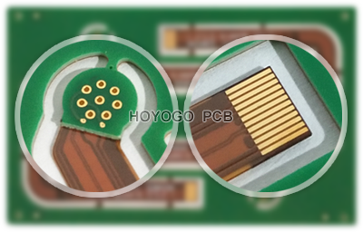
Requirements for Making Test Points of Rigid-flex Board
Key components need to preset test points on the rigid-flex board. However, the soldering pads of the assembled components are not allowed to be used as inspection points, and special test pads must be preset to ensure the normal progress of solder joint inspection and production debugging. The pads used for testing are made on the same side of the rigid and flexible board as much as possible, even if it is used for testing, it will help to reduce the cost of testing.

1. Process preset requirements for test points of rigid-flex boards
(1) The distance between the test points and the edge of the rigid-flex board must be greater than 5mm;
(2) The test point cannot be covered by solder mask or text ink;
(3) Test spot plating solder can choose a soft, easy to penetrate, and not easy to oxidize;
(4) The test point should be placed 1mm away from the component to prevent the probe and component from colliding;
(5) The test point needs to be placed 3.2mm outside the ring of the positioning hole, and the test point is used for accurate positioning. The error of the positioning hole should be within 0.05mm;
(6) The diameter of the test point should not be less than 0.4mm, and the distance between adjacent test points is preferably above 2.54mm and not less than 1.27mm;
(7) Components with a height exceeding 6.4mm cannot be placed on the test surface, components that are too high will cause poor contact between the line test fixture probe and the test point;
(8) The thickness, spacing and layout of the test point pads should also match the relevant requirements of the test equipment used.
2. Electrical preset requirements for test points of rigid-flex boards
(1) Try to lead the SMC/SMD test point on the component surface to the soldering surface through the via hole, and the diameter of the via hole is greater than 1mm;
(2) Each electrical contact needs to have a test point, and each IC needs to have a power and ground test point, and it should be as close to the component as possible, preferably within 2.54mm;
(3) When setting test points on the circuit trace, the width can be enlarged to 1mm;
(4) The test points should be evenly distributed on the PCB to reduce the probe pressure concentration;
(5) The power supply line on the PCB should be set with test breakpoints in different areas, so that the power supply can be decoupled or hindered to check.
HOYOGO is an international, professional, reliable rigid-flex PCB manufacturer. We have 2 factories production bases. Our production is strictly following high quality system of automotive products, we certified with ISO9001, ISO14001,ISO13485 and TS16949 and C-UL-S. All products strictly follow acceptance standard IPC-A-600-H and IPC-6012.
评论
发表评论