The Importance of PCB Heat Dissipation Design
In PCB design, heat dissipation is particularly important.
The heat generated by the electronic equipment can make the internal temperature rise rapidly, but if the heat is not dissipated in time, the equipment will continue to heat up, and the device will fail due to overheating, resulting in a decrease in the reliability of the product. At the source end of electronic design, we need to fully consider heat dissipation, which is especially important for PCB design planning for heat dissipation design.
The direct cause of the temperature rise of the PCB board is due to the existence of circuit power consumption devices, generally there are the following factors:
1. Unreasonable device selection, excessive electrical power consumption;
2. The radiator is not installed, resulting in abnormal heat conduction;
3. The PCB is partially unreasonable, causing local or overall temperature rise;
4. The heat dissipation design of PCB routing is unreasonable, which leads to heat concentration.
In view of common heat dissipation factors, we have proposed some common solutions for this factor when planning the heat dissipation design in PCB design:
1. Component Selection
When selecting models, low-power devices are preferred under the premise of achieving the same functions.
2. Component Placement Layout
Before the layout, we should start with the heat dissipation module from the schematic diagram, such as the common PMU module, DCDC module and some unit main control chips with relatively large heat dissipation. In the layout, we generally place these modules with large heat dissipation in blocks, and separate the non-severe heat dissipation modules with a distance of 3-5mm.
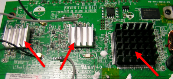
At the same time, if conditions permit, heat sinks can be added to the main control chip with severe heat dissipation for heat dissipation.

3. Heat Dissipation of PCB Routing
PCB good copper Routing is also an important way to strengthen heat dissipation:
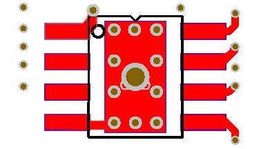
1.Adding a windowed through hole on the heat dissipation pad of the chip allows the heat dissipated by the chip to be introduced into a large copper surface through the through hole on the heat dissipation pad to disperse the heat, thus achieving the purpose of heat dissipation.

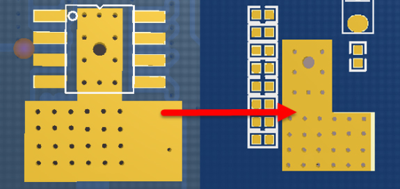
2.On the basis of drilling holes on the thermal pad, we can increase the heat dissipation area as much as possible. We can add open leaking copper on the front and back impedance layers, and add thermal open vias at the same time.

Analyzing the above factors from the PCB is an effective method to solve the temperature rise of the circuit board.These factors are usually interrelated in products and systems. Most factors should be analyzed based on actual conditions. Only in accordance with the specific actual situation can the problem be solved more correctly and the temperature rise can be reduced.
SHENZHEN HOYOGO ELECTRONIC TECHNOLOGY CO., LTD. has a professional PCB design and development team. In addition to independent research and development of various PCB solutions, we can also provide customers with a full range of services: including SMT assembly, PCB program development, schematic design, PCB Layout routing, Bom list matching, component procurement and other services.
评论
发表评论