ENEPIG Process
The ENEPIG (Electroless Nickel Electroless Palladium Immersion Gold) technology, is the addition of a layer of palladium between nickel and gold. In the deposition reaction of gold replacement, the electroless palladium layer protects the nickel layer from excessive corrosion by the replacement gold and is well prepared for immersion gold process.

ENEPIG process:
Degreasing ---- Microetch ---- Pickling ---- Pre-dip -----Activating Palladium ---- Chemical Nickel (Reduction) ---- Chemical Palladium (Reduction) ---- Chemical Gold (Replacement)
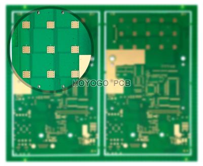
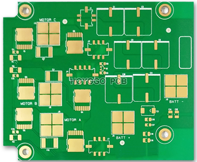
ENEPIG technology is applied to the surface treatment of package substrates. In the ENEPIG process, by controlling the palladium on the nickel layer and controlling the ENIG, accurate deposition thickness and uniformity of the gold layer are obtained to achieve a good contact surface. Through the comparison of wire bonding ability, solderability and aging resistance between ENEPIG pad and electroplated nickel gold pad, it is verified that ENEPIG has better wire bonding reliability than electroplated nickel gold and soldering reliability.
The deposited thickness of nickel is about 3 to 6 μm, the thickness of palladium is about 0.1 to 0.2 μm, and the thickness of gold is about 0.03 to 0.1 μm. ENEPIG control technology provides excellent surface treatment and meets all the requirements of lead-free assembly processes, making it ideal for surface-handling of packaged substrates.

In 2000, ENEPIG was delayed in the market because palladium metal prices were speculatively sold to unreasonably high prices. However, because ENEPIG can solve the reliability problems of many new packages and meet the requirements of ROHS, it was later paid attention to by the market. Companies that currently use this process: Microsoft, IPhone, Intel and so on.
The advantages of ENEPIG are detailed below:
1. It can prevent the occurrence of "black nickel problem", and there is no phenomenon in which the surface of nickel is attacked by gold to form grain boundary corrosion.
2. Electroless palladium plating acts as a barrier layer and does not cause copper migration to the gold layer, resulting in poor solderability.
3. The electroless palladium layer is completely dissolved in the solder and there is no high phosphor layer on the alloy interface. At the same time, when the electroless palladium is dissolved, a new layer of electroless nickel is exposed to form a good nickel-tin alloy.
4. It can withstand multiple lead-free reflow cycles.
5. Excellent combination of gold wire.
6. In general, its total production cost is lower than electroplated nickel gold, electroless nickel plating and electroless gold plating.

评论
发表评论