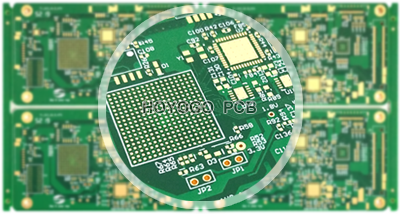
The Multilayer Circuit Board Production Process
First: The Purpose of Blackening and Browning
1. Remove pollutants such as oil and impurities on the surface;
2. Increase the specific surface area of the copper foil, thereby increasing the contact area with the resin, which is conducive to the full diffusion of the resin and the formation of greater bonding force;
3. Turn the non-polar copper surface into a polar CuO and Cu2O surface to increase the polar bond between the copper foil and the resin.
4. The oxidized surface is not affected by high temperature and humidity, thereby reducing the chance of delamination between the copper foil and the resin.
5. Circuit boards with internal circuits must be blackened or browned before being laminated. It is to oxidize the copper surface of the inner board. Generally, the produced Cu2O is red and CuO is black, so the Cu2O-based oxide layer is called browning, and the CuO-based oxide layer is called blackening.
Laminating is the process of bonding each layer of the circuit into a whole through B-grade prepreg. This bonding is achieved through mutual diffusion and penetration between macromolecules on the interface, and then interweaving.
Purpose: To press the discontinuous multilayer board and the adhesive board into a multilayer board with the required number of layers and thickness.

1. The layout combines copper foil, adhesive board (prepreg), inner layer board, stainless steel, isolation board, kraft paper, outer layer steel board and other materials according to process requirements. If the circuit board has more than 6 layers, pre-Layout is also required.
2. The lamination process sends the stacked circuit boards into a vacuum heat press. The heat energy provided by the machine is used to melt the resin in the resin sheet to bond the substrate and fill the gap.
3. For designers, the primary consideration for lamination is symmetry. Because the board will be affected by pressure and temperature during the extrusion process, there will be stress inside the board after the extrusion is completed. So, if the 2 sides of the laminate are not uniform, the stresses on the two sides will be different, causing the laminate to bend to one side, which greatly affects the performance of the PCB.
In addition, even in the same plane, if the copper distribution is uneven, the resin flow speed at each point will be different. In this way, the thickness will be thinner where there is less copper, and the thickness will be thicker where there is more copper. In order to avoid these problems, various factors must be carefully considered in the design process, such as the uniformity of copper distribution, the symmetry of the laminate, the design and layout of blind and buried vias, etc.
Second: Decontamination and Electroless Plating Copper
Purpose: To metalize the via.
1. The substrate of circuit board is composed of copper foil, fiberglass and epoxy resin. In the production process, the hole wall section after drilling the base material is composed of the above three parts of materials.
2. Hole metallization is to solve the problem of covering a uniform heat-resistant copper layer on the cross section.
3. The process is divided into 3 parts: the first part is the drilling process, the second part is the electroless copper plating process, and the third part is the thick copper process (copper plating on the entire board).
Third: Electroless Plating Copper and Thickened Copper
Hole metallization involves the concept of capacity: the ratio of thickness to diameter. The ratio of thickness to diameter refers to the ratio of board thickness to aperture. With the continuous thickening of the plate and the continuous reduction of the hole diameter, it becomes more and more difficult for the chemical solution to enter the drilling depth. Although the electroplating equipment uses vibration, pressure, and other methods to get the syrup into the center of the drilled hole, it is inevitable that a thinner center plating layer caused by the concentration difference will occur. At this time, there will be a slight open circuit phenomenon in the drilled layer. When the voltage rises and the circuit board is impacted under various harsh conditions, the defects will be completely exposed, which will cause the circuit board to break and fail to complete the specified work.
So, designers need to know the process capability of the circuit board manufacturer in time, otherwise the designed PCB will be difficult to realize in production. It should be noted that not only in the design of vias, but also in the design of blind vias and buried vias, the parameter of the ratio of thickness to diameter must be considered.
Fourth: Outer Dry Film and Pattern Plating
The principle of outer layer graphics transmission is similar to the principle of inner layer graphics transmission. Both use photosensitive dry film and photographic methods to print circuit patterns on the board. The difference between outer dry film and inner dry film is:
If subtraction is used, the outer dry film is the same as the inner dry film, and the negative film is used as the board. The cured dry film part of the circuit board is the circuit. The uncured film is removed, and the post-processing is performed after acid etching, and the circuit pattern remains on the board due to the protection of the film.
评论
发表评论