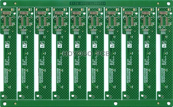
Why do PCB Need Panelization?
Generally, before PCB design or production, a PCB panelization operation will be carried out, and after the processing is completed, it needs to be cut into single board. So why do it?

The track of the SMT placement machine has a maximum and minimum size limit. When using 1 pcs smaller size PCB for processing, although it can sometimes pass the track of the placement machine, it wastes the capacity of the placement machine and the production efficiency is not high. However, if there are 10pcs, 20pcs, etc. single PCB in the panel, this will not only improve the welding efficiency of the patch, but also only need to pass the placement machine once to complete the welding of multiple PCB.
After the PCB processing is complete, a lot of testing needs to be done. Such as burn-in test, programming test, ICT test, signal test, etc. Then it has more circulation time in the production workshop, and it is also a big problem for the storage space after SMT processing. If it is a panelization storage, the tray does not need a lot, and in the test can be done with the connecting board when testing, and it can also save the time wasted when picking and placing in the jig.
To sum up, the PCB panelization not only improves the production efficiency, but also saves a lot of time and cost. SHENZHEN HOYOGO ELECTRONIC TECHNOLOGY CO., LTD. is a professional and reliable PCB manufacturer, including one-stop PCB service from upstream electronic components procurement to PCB production and processing, SMT placement, PCBA testing, finished product assembly, etc.
评论
发表评论