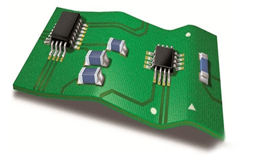
What Causes PCB Warpage?
PCB warpage refers to the problem that the substrate appears as a plane unevenness during the PCB manufacturing process. This problem can lead to poor electrical connections, damaged components, signal interference, and more. Therefore, enough attention should be paid to the problem of PCB boards warpage. So what is the PCB warpage standard? What causes PCB warpage?

I. PCB Warpage Standard
The PCB industry attaches great importance to the problem of PCB warpage, so it also stipulates some warpage standards and clarifies the specific numerical requirements for warpage. The current standard for PCB warpage is mainly the IPC-6012 specification.
The IPC-6012 specification is a general specification adopted by the PCB industry, which mainly stipulates the following standards:
1) Single sided or double sided boards cannot exceed 0.75% of the size;
2) Multi-layer boards cannot exceed 0.50% of the size.
II. Causes of PCB Warpage
The appearance of PCB warpage is often the result of a combination of various factors. Here are some common causes that may cause PCB warpage:
1. Material Problem: The materials of the substrate and the pad do not match, the material batches are different, the glue is uneven, etc.
2. Technology Problem: Improper technology in different links during PCB processing, such as copper foil silver plating, uneven etching, assembly, etc.
3. Design Problem: PCB design may have problems such as improper wiring, unreasonable device layout, and unequal positions of resistors and capacitors.
4. Temperature Problem: During PCB processing, the temperature changes greatly, or there are problems such as thermal stress concentration and uneven cooling.
5. Thickness Problem: During the process of bare board and pad processing of PCB, the thickness of different layers does not match, and the thickness changes greatly.
In addition to the warpage limit stipulated in the IPC-6012Cstandard, it is necessary to judge and control according to the specific situation in actual application. For example, for some special application scenarios, such as high-end fields such as aerospace and military equipment, the requirements for PCB warpage will be more stringent, and more precise control and detection are required.
HoYoGo is an international, professional and reliable PCB manufacturer. Our minimum PCB warpage can reach <0.3%, and all products are strictly in accordance with IPC-A-600-H and IPC-6012 acceptance standards, which can guarantee the quality and reliability of each product delivered to customers.
评论
发表评论