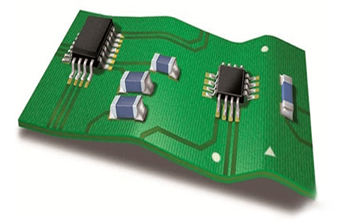
How to Avoid PCB Warpage
When the PCB is deformed, it is easy to cause problems such as poor circuit connection, component damage, signal interference, etc., and may even seriously threaten the quality and performance of the entire product. So how can we avoid PCB warping?

1. Design Stage
1) Reasonable layout of components
We should try to avoid large components concentrated in the same area, forming a huge tension difference with other small components. This can effectively reduce the PCB warpage problem caused by local stress.
2) Control the thickness of copper foil
The thickness of the copper foil in the PCB will also affect its warpage. Therefore, we need to make reasonable planning at the design stage, and control the thickness of each layer of copper foil to be as uniform as possible.
2. Manufacturing Stage
1) Control manufacturing temperature and humidity
Heating and cooling are unavoidable steps in the PCB manufacturing process. But these steps need to control the temperature and humidity, avoid too high or too low. Especially for multi-layer PCB boards, it is necessary to control the pressure balance between layers to avoid stress concentration problems.
2) Choose high-quality materials
The PCB warpage problem also has a lot to do with the quality of the material. Therefore, we should try our best to choose some high-quality materials to make PCB. For example, in terms of glass fiber content, we can choose glass fiber cloth with a higher content, which can effectively improve the strength and stability of the PCB board.
3. Verification Stage
1) PCB inspection
After the PCB is manufactured, we need to carry out strict testing. Observe the deformation of the PCB by means of X-ray flaw detection and 3D scanning. If problems such as warping are found, they need to be repaired and adjusted in time.
2) Monitor PCB during use
Even if the PCB board has been strictly manufactured and tested, we also need to monitor it during use. For example, before testing the product, CT detection can be performed on the PCB board to ensure that there is no warpage problem. If the PCB board is found to be deformed during use, it needs to be checked, repaired and improved in time.
Although the occurrence of PCB warpage problem is often the result of a combination of various factors, we can avoid PCB warpage problems as much as possible, and improve reliability and stability of the overall product through control and adjustment in multiple stages such as design, manufacturing, and verification.
HoYoGo as an international, professional and reliable PCB manufacturer. Our minimum PCB warpage can reach <0.3%, and all products are strictly in accordance with IPC-A-600-H and IPC-6012 acceptance standards, which can guarantee the quality and reliability of each product delivered to customers.
评论
发表评论