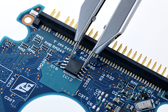
The Silkscreen on the PCB Have Such a Big Meaning
PCB silkscreens are a process that is printed on the PCB board for marking, which is convenient for finding the tag number of each component during assembly, and finding the corresponding position of each component during maintenance. These silkscreens are essential for PCBA factory to participate in circuit board assembly, testing or troubleshooting. So what are the PCB silkscreens? What does it mean?

1. Component Identifier
Component identifiers are letters or numbers that identify specific components on a PCB, such as resistors, capacitors, and integrated circuits.
2. Reference Mark
Reference marks are used to identify the function of each component or circuit on the PCB, such as "R" for resistors and "C" for capacitors.
3. Trace Mark
Trace mark are lines or symbols that indicate the path of electrical traces on a PCB board and are used to connect various components and circuits.
4. Silkscreen Label
Silkscreen labels refer to text or graphics printed on PCB to provide additional information about a design, such as a company logo or part number.
5. Test Point
A test point is a location on a PCB where test equipment can be connected to measure voltage, current, or other electrical parameters.
6. Component Value Mark
In addition to component codes, some PCB will contain marks indicating specific component values. For example, a resistor might be marked with a code indicating its resistance value, or a capacitor might be marked with its capacitance value and rated voltage.
7. Pin Number
Many components on a PCB have multiple pins, and the pin numbers may be marked to indicate the order in which they are connected to the circuit.
8. Polarized Mark
Certain components have polarity, such as capacitors or diodes. These polarities must be observed when mounting them on the PCB. The PCB may contain markings such as plus or minus signs or arrows to indicate the correct orientation of these components.
HOYOGO is an international, professional and reliable PCBA factory. The management team has an average of 25 years of industry experience. We also have 2 factory production bases with a monthly production capacity of 500,000 square meters. With our rich experience, production capacity and resources, we can provide you with one-stop service from small to mass production.
评论
发表评论