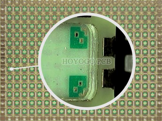
What are the Advantages of PCB Step Slots
PCB step slots are a special design on PCB that creates a series of slots or steps of different heights along the edges or specific areas inside the PCB. These slots are usually made up of stacked layers, creating the ladder-like structure of the PCB. Do you know what are the advantages of PCB step slots?
1. Electromagnetic interference control
The step slots create ground planes of different heights in the PCB, which can effectively isolate electromagnetic interference between different signal layers, thereby improving the signal integrity and performance stability of the circuit board.
2. Signal integrity
Step slots can reduce crosstalk and coupling between different signal layers in the PCB. By creating a height difference in the PCB, step slots can prevent signals from traveling from one place to another, thereby reducing the adverse effects caused by signal interconnection.
3. Manage heat
Step slots can also be used to better manage heat in the PCB. By creating thermal insulation layers of different heights in the PCB, step slots can provide better heat dissipation, thereby reducing the temperature of electronic components and improving the stability and reliability of the device.
4. Space optimization
In PCB design, step slots can be used for space optimization. By cleverly designing and placing step slots, layout and routing can be effectively done in a limited space, improving the density and performance of the circuit board.
HoYoGo is an international, professional and top 15 PCB manufacturer in China. We can meet customer’s requirements for PCB step slot technology. At the same time, HoYoGo also has an excellent and stable quality system that supports various complex technologies, such as customized lamination structures, large-size boards, ENEPIG technologies, etc. If you have related needs, you are welcome to send us inquiries.

评论
发表评论