Detailed Explanation of the Meaning of Each Layer of PCB Gerber File
For entry-level electronics engineers, especially those unfamiliar with PCB prototyping process, the first time they hear terms like "Gerber file", "solder mask opening", "green/black solder mask", "stencil manufacturing" or "exporting Gerber files to the PCB manufacturer," they may feel confused or overwhelmed. This article focuses on explaining the meaning and functions of each layer in a PCB Gerber file, helping beginners understand the structure and purpose, and preparing them for future prototyping.
1. How to Export Gerber Files
After completing the PCB layout design and passing the DRC (Design Rule Check), you can proceed to export the Gerber files.
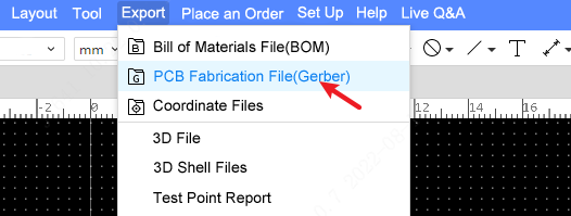
There are typically two ways to export Gerber files:
(1) One-Click Export
Exports all layers and graphic primitives based on default settings. It does not include drill tables or separate drill information files.
(2) Custom Configuration
You can customize the configuration as needed, including:
* Supporting drill information and drill tables;
* Adding multiple configurations to the list on the left;
* Selecting the layers to export;
* Mirroring layers;
* Choosing the specific graphic primitives objects to export;
* When exporting Gerber files, select a configuration to proceed.
For most typical applications, the default one-click export is sufficient, with no need to adjust custom configurations. Note that different PCB design software, such as Altium Designer, KiCad, EasyEDA, etc. all support Gerber file export, although the specific steps may vary slightly. Detailed instructions for each software are not covered here.
2. Gerber File Analysis
When analyzing Gerber files, common DFM (Design for Manufacturability) tools or CAM (Computer-Aided Manufacturing) software, such as Gerber viewers or PCB fabrication utilities, can be used to inspect the design data on each layer. These tools provide a clear understanding of what each layer represents and how it corresponds to the physical structure of the final PCB.
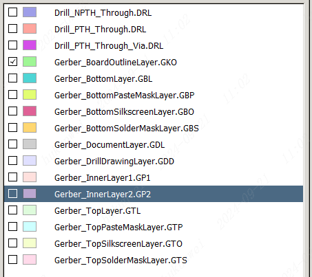
Layer Table Description:
Filename | Type | Remarks / Explanation |
Drill_PTH_Through | Plated Through Hole Drill Layer | Drills hole positions requiring plating of the inner wall, such as multilayer pads and vias. |
Drill_PTH_Through_Via | Plated Through Hole Via Drill Layer | Positions for holes requiring plating on inner walls, such as vias. |
Drill_NPTH_Through | Non-Plated Through Hole Drill Layer | Drill holes with non-plated through holes (NPTH), where the inner walls are not metallized, such as circular cutout areas. |
Drill_PTH_Inner1_to_Inner2 | Drilling layers for metallized blind and buried vias | Drill holes with metallized inner walls. Inner1 and Inner2 layers adjust automatically based on blind and buried via types. As this design does not use blind or buried vias, no Gerber files are generated for these layers. |
BoardOutline | Board Outline File | Cut the board shape according to this file |
Top / BottomLayer | PCB Top / Bottom Layer | Top/bottom copper foil layer |
Gerber_InnerLayer1 | Inner Copper Layer | Signal layer type |
Gerber_InnerLayer2 | Inner Copper Layer | Inner layers of the inner electrical layer type are output as positives in the Gerber files, while during PCB design they are drawn as negatives (lines drawn are not included in the Gerber output). |
Top/BottomSilkLayer | Top / Bottom Silkscreen Layer | Component numbers and characters seen on the PCB |
Top/Bottom SolderMaskLayer | Top / Bottom Solder Mask Layer | It can also be called the solder mask opening layer. By default, the board is covered with solder mask (commonly green or other colors). Elements drawn on this layer correspond to areas on the top layer where the solder mask is not applied. |
Top/Bottom PasteMaskLayer | Bottom Solder Paste Layer | Used for stencil fabrication, a metal sheet is cut to create openings at the pad locations. When the stencil is aligned over the PCB, solder paste is applied only to the exposed pad areas through these openings. |
MechanicalLayer | Mechanical Layer | This layer stores information recorded in the mechanical layer of the PCB design and is used for documentation purposes only. By default, its shapes are not used in manufacturing. It serves primarily as a reference for text annotations, such as process parameters, V-cut paths, etc. |
DocumentLayer | Documentation Layer | Used to record PCB annotation information; not involved in manufacturing. |
DrillDrawingLayer | Drill Drawing Layer | This layer is not used in manufacturing and serves only as a reference to mark the locations of generated vias. |
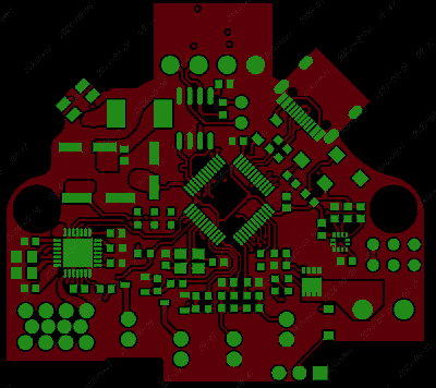
3. Intuitive Analysis
Below is an analysis of the Top Silkscreen, Solder Mask, Solder Paste, and Top Copper layers to form an intuitive understanding.
2D Simulation Top Layer View:
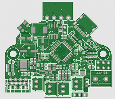
Top Copper Layer:
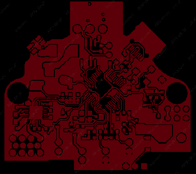
Top Solder Mask Layer (Green Area):
The solder mask layer is also commonly referred to as the “solder mask opening layer” or “green solder mask layer”. It defines the areas on the PCB that will be covered with solder mask ink (typically green). In design files, the solder mask layer is output as a negative image—that is, the patterns visible in the solder mask layer actually indicate the regions on the finished board that will not be covered with solder mask, leaving the copper exposed. These exposed areas are usually pads, vias, or other spots that require soldering, which is why they are commonly referred to as “solder mask openings”.
In other words, the green areas in this image will not be covered with ink, while the areas without green will be covered. This can also be confirmed by comparing it with the simulation diagram. The paste mask layer, also known as the solder paste layer, is shown in blue in the following image:
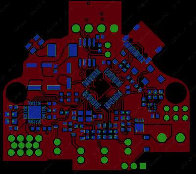
The blue areas indicate where solder paste will be applied. These regions are slightly smaller than those on the solder mask layer at the same pad locations.
Top Silkscreen Layer:
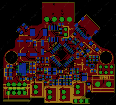
The yellow areas represent the Silkscreen Layer.
It’s important to highlight the bottom silkscreen layer here. As shown in the Gerber file below, the layer appears mirrored in the preview, this is expected behavior. Since the silkscreen is printed from the bottom side of the PCB, it must appear mirrored in the Gerber preview in order to appear correctly on the final physical board.
This is similar to how components and silkscreen elements on the bottom layer appear mirrored when viewed in PCB layout software. Conversely, if the bottom silkscreen appears in normal (non-mirrored) orientation in the Gerber preview, it will end up being printed in reverse on the actual board, which is incorrect.
4. Summary
After introducing the main Gerber layers, this article does not further illustrate via layers or additional inner/bottom layers. Readers are encouraged to open a real Gerber file (exported from your PCB design) for self-analysis and better understanding. Once the Gerber file analysis is complete, it can be submitted to the board manufacturer for prototyping. For mass production, it is recommended to perform a Design for Manufacturability (DFM) check to ensure production consistency and stability.
Gerber Files for Different PCB Layer Counts
For Gerber files, multi-layer PCBs contain more internal layer data compared to single-layer or double-layer boards. These internal layers define signal routing layers, power planes, and ground planes, serving as the foundation for high-density routing and complex circuit functionality.
Comparison of PCBs with Varying Layer Counts
The following is a brief comparison of common PCBs with different layer counts (such as 1-layer, 2-layer, 4-layer, 6-layer, 8-layer and above) in terms of performance and application.
(1) Layer Count and Routing Capability
Multi-layer PCBs (usually 4 layers and above) support higher routing density and complex designs, making them suitable for high-speed, high-frequency applications. In contrast, single- and double-layer PCBs are limited in routing capability and are used for simpler, low-speed systems.
(2) Electrical Performance
Multi-layer PCBs offer superior electrical performance. With well-designed power and ground planes, they can effectively reduce signal crosstalk, improve electromagnetic compatibility (EMC), and enhance signal integrity. In contrast, single- and double-layer PCBs are limited in these aspects and are less suitable for high-reliability or high-speed signal applications.
(3) Thermal Management Capabilities
Multi-layer PCBs can achieve optimized heat dissipation paths through inner-layer routing and copper foil design, making them suitable for electronic products with high power density or significant thermal management requirements. In contrast, single-layer and double-layer PCBs have limited heat dissipation capabilities and primarily rely on external heat sinks or thicker copper traces.
(4) Manufacturing Process & Cost
The manufacturing process of multi-layer PCBs is more complex, such as lamination, blind and buried vias, via-in-pad, which results in higher production costs. In contrast, single-layer and double-layer PCBs have simpler structures and mature fabrication processes, offering shorter lead times and lower costs, making them suitable for cost-sensitive projects and high-volume production.
In summary, PCBs with different layer counts exhibit significant differences in routing capability, electrical performance, thermal management, and manufacturing process complexity. Multi-layer PCBs are well-suited for applications that require complex functionality, limited space, and high performance, while single-layer and double-layer PCBs are more appropriate for simpler designs where cost control is a primary concern.
SHENZHEN HOYOGO ELECTRONIC TECHNOLOGY CO., LTD. is a professional and reliable PCB manufacturer. We provide customers with one-stop services from upstream electronic component sourcing to PCB production and processing, SMT assembly, PCBA testing, and final product assembly. If you have related needs, you are welcome to cend us an inquiry.


评论
发表评论