What Is an Optical Module PCB
Optical modules are essential components for high-speed optical communication systems and are widely deployed in data center switches, server clusters, and telecommunications network equipment. Driven by the rapid growth of AI computing and increasing network bandwidth demands, the adoption of high-speed optical modules continues to expand, placing greater demands on the performance and reliability of the PCBs used within them.
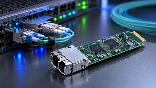
An Optical Module PCB is a specialized printed circuit board designed for use inside optical transceivers and optical communication modules. It serves as the mounting platform for critical components such as driver ICs, controller ICs, power management devices, connectors, and optoelectronic components, providing reliable mechanical support and electrical connectivity. As the foundation of the module's electronic architecture, the PCB enables high-speed signal transmission, efficient power distribution, and reliable interconnection among various functional modules.
Although optical-to-electrical and electrical-to-optical conversion, signal modulation, and data processing are primarily performed by semiconductor chips and optical devices, the design and manufacturing quality of the PCB have a direct impact on the overall performance and reliability of the optical module. In high-speed optical modules operating at 100G, 400G, 800G, and beyond, the PCB is no longer just a passive carrier. It has become a critical component for maintaining signal integrity, minimizing transmission loss, and ensuring stable high-speed data transmission.
The Role of Optical Module PCBs in Optical Modules
Optical modules integrate a variety of components, including driver ICs, DSP ICs, power management devices, and optical components, all of which are mounted and interconnected on the PCB to form a complete functional system. In addition to providing mechanical support, the PCB establishes electrical interconnections within the module. Through precisely engineered circuit traces, it connects various components, enabling high-speed data transmission and reliable operation.
Although functions such as optical-to-electrical and electrical-to-optical conversion, signal processing, and data transmission are primarily performed by integrated circuits and optical components, the design and manufacturing quality of the PCB directly affect the module's performance, reliability, and stability. As a result, the optical module PCB has become a critical foundation for ensuring the stable and reliable operation of optical modules.
Technical Characteristics of Optical Module PCBs
Compared with conventional PCBs, optical module PCBs typically need to meet higher requirements for data transmission performance and reliability. To support the high-speed communication requirements of 100G, 400G, and 800G optical modules, these PCBs typically incorporate precise impedance control, high-speed differential routing, and optimized stack-up designs. In certain high-speed applications, low-loss materials and HDI (High-Density Interconnect) technology are also employed to reduce signal loss and improve routing density.
In addition, optical modules are often required to operate for extended periods in data center and telecommunications network environments. Therefore, the PCB must exhibit excellent thermal stability, batch-to-batch consistency, and long-term reliability.
Background of Optical Module PCB Development
The rapid growth of data center interconnects, cloud computing platforms, and AI computing clusters is driving the evolution of optical modules toward higher data rates. Optical module data rates have progressed from 10G, 25G, and 40G to 100G, 200G, and 400G. Today, 800G optical modules are being deployed at scale, while the adoption of 1.6T optical modules is gaining momentum.
As optical module data rates continue to increase, the complexity of internal electronic systems also grows, placing higher requirements on PCB signal integrity, reliability, and manufacturing precision. As a result, optical module PCBs have become a critical and indispensable part of the optical communications ecosystem.
Primary Applications of Optical Module PCBs
Optical module PCBs are widely used in a wide range of high-speed optical communication systems, including the following:
1) Data center switches and server interconnect systems;
2) Cloud computing infrastructure;
3) AI servers and GPU computing clusters;
4) Telecom backbone networks;
5) Metro and access network equipment;
6) Enterprise networking equipment;
7) High-performance computing (HPC) systems.
Growing AI Computing Demand Drives Demand for Optical Module PCBs
Large-scale AI model training and inference require massive GPU and AI accelerator clusters to handle highly parallel workloads. These workloads depend on high-speed interconnect networks for data exchange between computing nodes.
In large-scale AI clusters, data transmission between servers increasingly relies on high-speed optical modules. As AI data centers and computing clusters continue to expand, deployments of 400G and 800G optical modules are growing rapidly, further driving demand for high-performance optical module PCBs.
Looking ahead, AI computing networks are expected to evolve toward higher-bandwidth architectures, further increasing demand for high-speed, high-reliability PCB products.
Reliability Requirements for Optical Module PCBs
Data centers and telecommunications networks typically operate 24/7 year-round. A failure in a single optical module may affect overall network stability. Under such operating conditions, the long-term stability and manufacturing consistency of the PCB become particularly important.
Therefore, in addition to supporting high-speed signal transmission, optical module PCBs must also exhibit:
1) Excellent long-term stability;
2) Strong thermal reliability;
3) Stable electrical performance;
4) Batch-to-batch consistency in mass production;
5) Manufacturing processes compliant with relevant IPC standards.
For high-speed optical communication systems, high reliability has become one of the key technical criteria for optical module PCBs.
Data center upgrades, the expansion of AI computing infrastructure, and the advancement of high-speed networking technologies are continuously driving optical modules toward higher bandwidth and greater integration density. As a critical electronic interconnection platform within optical modules, the PCB not only provides component mounting and electrical interconnection, but also directly affects signal integrity and overall system reliability.
As 400G, 800G, and emerging 1.6T optical modules continue to evolve, high-performance and highly reliable optical module PCBs will become increasingly important. This trend is expected to further drive demand for high-reliability PCBs and communication PCBs.
HoYoGo is an international, professional, and reliable optical module PCB manufacturer, providing one-stop services covering the entire supply chain, including upstream electronic component sourcing, PCB fabrication, SMT assembly, PCBA testing, and final product assembly. All products are manufactured and quality-controlled in strict compliance with IPC-A-600 and IPC-6012 standards, ensuring high-reliability PCB solutions for optical communications, data centers, and AI infrastructure applications. If you are looking for a trusted PCB manufacturing partner, please feel free to contact us for more information or a competitive quotation.


评论
发表评论